- The CMOS transmission gate consists of one nMOS and one pMOS transistor, connected in parallel.
- The gate voltages applied to these two transistors are also set to be complementary signals.
- Thus, the CMOS TG operates as a bidirectional switch between the nodes A and B which is controlled by signal C.
- If the control signal C is
- logic-high, i.e., equal to VDD, then both transistors are turned on and provide a low-resistance current path between the nodes A and B.
- low, then both transistors will be off, and the path between the nodes A and B will be an open circuit. This condition is also called the high-impedance state.
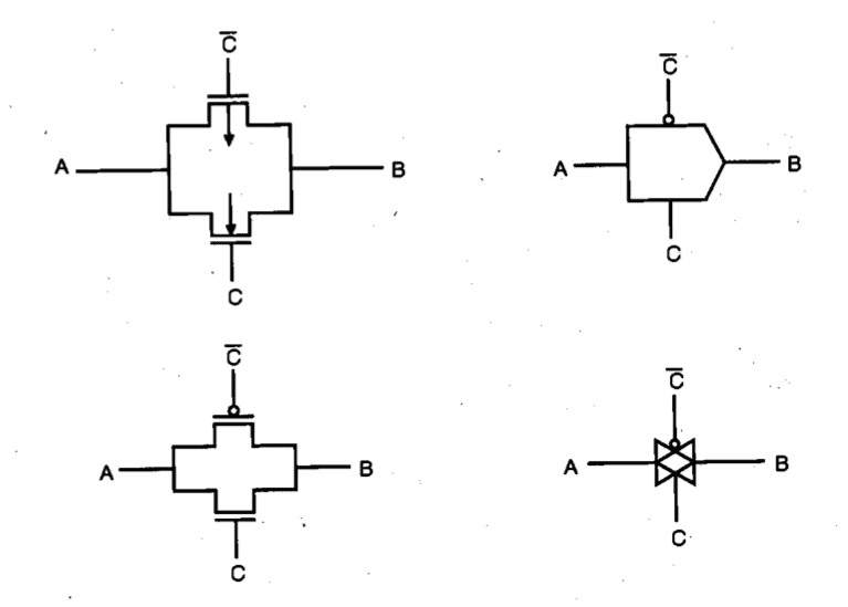
- The NMOS switch passes a good zero but a poor 1.
- The PMOS switch passes a good one but a poor 0.
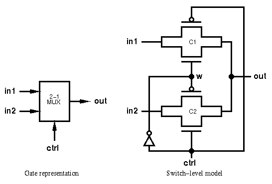
- TGs are efficient in implementing some functions such as multiplexers, XORs, XNORs, latches, and Flip-Flops.
- For a detailed DC analysis of the CMOS transmission gate, we will consider the following bias condition
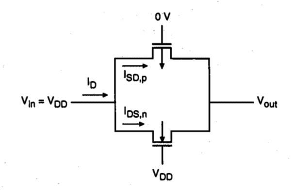
- The input node (A) – constant logic-high voltage, Vin = VDD.
- The control signal (C) – logic-high (ensuring that both transistors are turned on.)
- The output node (B) – connected to a capacitor (capacitive loading of the subsequent logic stages driven by the transmission gate.)
6.1 The input-output current-voltage relationship of the CMOS TG as a function of the output voltage Vout
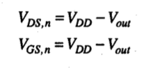
- For nMOS Transistor:
-
- Thus, nMOS turned off = Vout > VDD – VT,n
- nMOS operate in saturation region = Vout < VDD – VT,n
- (VT,n – nMOS Transistor threshold voltage)
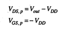
- For pMOS Transistor:
-
- pMOS operate in linear region = Vout > | VT,p |
- (VT,p – pMOS Transistor threshold voltage)
- pMOS in saturation region = Vout < | VT,p |
Thus, unlike the nMOS transistor, pMOS transistor remains turned on, regardless of the output voltage level Vout.
6.2 The total current flowing through the transmission gate is the sum of the nMOS drain current and the pMOS drain current.
![]()
6.3 Equivalent Resistance for each transistor:
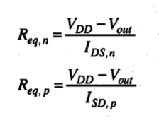
- Three operating regions for the CMOS transmission gate, depending on the output voltage level:
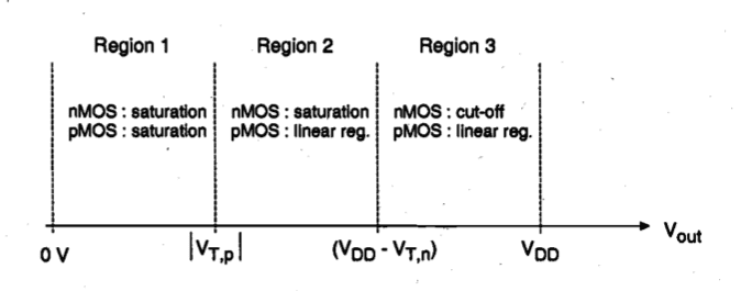
- Region 1: Both nMOS and pMOS in saturation and Vout < | VT,p |
- Region 2: nMOS in saturation, pMOS in linear region and | VT,p |< Vout < (VDD – VT,n)
- Region 3: nMOS cut off (or off), pMOS in linear region and Vout > (VDD – VT,n)
- Plot: total resistance of the CMOS transmission gate as a function of the output voltage (Vout):
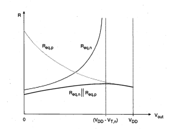
Thus, the total equivalent resistance of the TG remains relatively constant, i.e., its value is almost independent of the output voltage, whereas the individual equivalent resistances of both the nMOS and the pMOS transistors are strongly dependent on Vout. This property of the CMOS TG is naturally quite desirable.
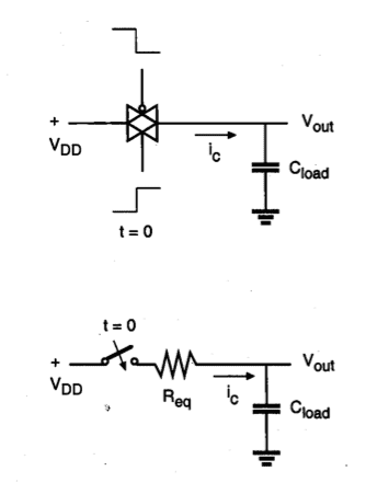
- A CMOS pass gate which is turned on by a logic-high control signal can be replaced by its simple equivalent resistance for dynamic analysis, as shown below:
- Advantages:
- There is no degradation in the o/p logic level.
- It is more sensitive.
- Less Propagation Delay.
- Disadvantages:
- Requires both nMOS and pMOS in different wells.
- Both true and complemented polarities of the control signal needed.
- Parallel connection of both transistors increases node capacitance.
STRUCTURES USING CMOS TRANSMISSION GATE:
References: CMOS DIGITAL INTEGRATED CIRCUITS ANALYSIS & DESIGN
I want to design 4×1 mux by using CMOS ?
i want to design 1:8 demux using cmos?