- Latch-up is defined as the generation of a low-impedance path in CMOS chips between the power supply (VDD) and the ground (GND) due to the interaction of parasitic PNP and NPN bipolar junction transistors (BJTs).
- These BJTs form a silicon – controlled rectifier (SCR) with positive feedback and virtually short circuit VDD to the ground, thus causing excessive current flows and even permanent device damage.
- Latch-up occurs when:
- When both BJTs conduct, creating low resistance path between VDD and GND.
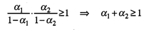
- Product of gain of two transistors in the feedback loop is greater than one (β1 x β2 ≥ 1)
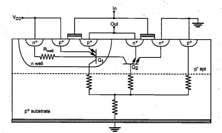
Fig: Cross-sectional view of a CMOS inverter with parasitic bipolar transistors
- In the equivalent circuit:
- Q1: vertical bipolar PNP transistor whose base is formed by the n-well with its base-to-collector current gain (β1) as high as several hundred. It is associated with pMOS.
- Q2: lateral bipolar NPN transistor whose base is formed by the p-type substrate with its base-to-collector current gain (β2) ranging from few tenths to tens. It is associated with nMOS.
- Rwell: the parasitic resistance in the n-well structure with its value ranging up to 20kΩ.
- Rsub: substrate resistance that strongly depends on the substrate structure with its value ranging from several hundred to few ohms.
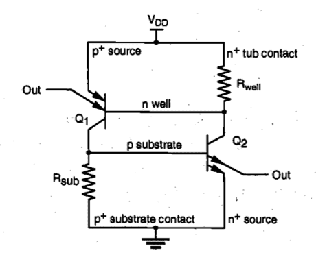
Fig: Circuit model for SCR formed of parasitic BJTs
- Operation:
- First of all, assume that the Rwell and Rsub are sufficiently large so that they can be neglected (open circuit).
- Now unless SCR is triggered by an external disturbance, the collector current of both transistors consists of the revenge leakage currents of the collector-base junction and therefore, their current gains are very low.
- If the collector current of one of the transistors is temporarily increased by an external disturbance, however, the resulting feedback loop causes this current to be multiplied by (β1β2). This event is called triggering of the SCR.
- Once triggered, each transistor drives the other transistor with positive feedback, eventually creating and sustaining a low-impedance path between VDD and GND, resulting in latch-up.
- If the condition, β1 x β2 ≥ 1 is satisfied, both transistors will continue to conduct a high (saturation) current, even after triggering is not there. (β is base to collector current gain).
- In terms of collector-emitter current gain, the latch-up condition given as:
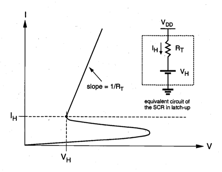
- At the onset of latch-up, voltage drop across the SCR becomes
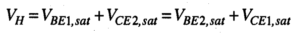 where,
VH = holding voltage
IH = holding current - The low impedance state is sustained as long as the current through SCR is greater than IH(holding current), which is determined by the device structure.
- Also note that the slope of the I-V curve is determined by the total parasitic resistance in the current path, RT.
Thank you for very informative post.