Terminology:
- IDS = current from drain to source OR drain-source current
- VDS = drain to source voltage
- L = length of the channel
Now for the ideal case, in the saturation region, IDS becomes independent of VDS i.e. in the saturation region channel is pinched off at the drain end and a further increase in VDS has no effect on the channel’s shape.
But in practice increase in VDS does affect the channel. In the saturation region, when VDS increases, the channel pinch-off point is moved slightly away from the drain, towards the source as the drain electron field “pushes” it back. The reverse bias depletion region widens and the effective channel length decreases by an amount of ∆L for an increase in VDS.
Thus the channel no longer “touches” the drain and acquires an asymmetrical shape that is thinner at the drain end. This phenomenon is known as channel length modulation.
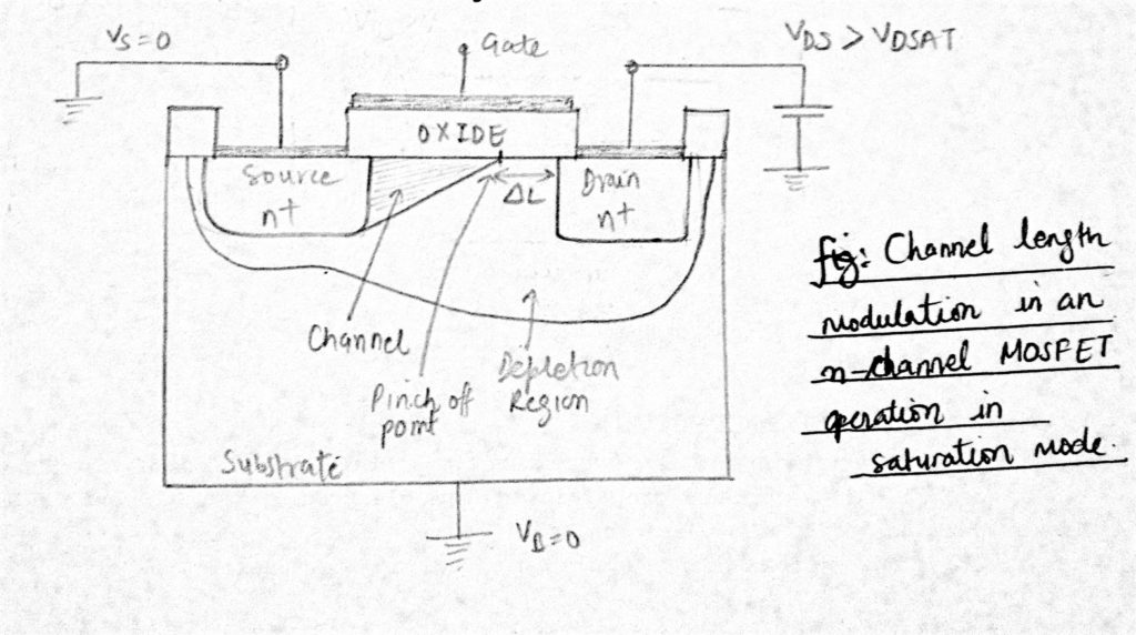
In large devices, this effect is negligible but for shorter devices ∆L/L becomes important. Also in the saturation region due to channel length modulation, IDS increases with increase in VDS and also increases with the decrease in channel length L.
The voltage-current curve is no longer flat in this region.
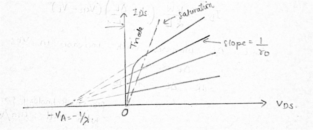
The drain current with channel length modulation is given by:

DERIVATION:
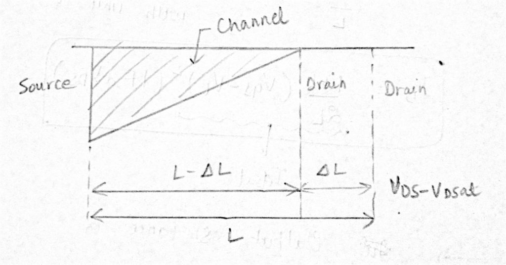
To account for the dependence of ID on VDS in the saturation region, replace L by L – ∆L. We know that in the saturation region, drain to source current (IDS = ID) is given by:


Assuming 

Since ∆L increases with increase in VDS

OR

where,  = process technology parameter with unit μm/V.

therefore,

where,
 = process technology parameter with unit V-1

sir i still don”t understand when it said that channel length modulation occurs when vds is higher than vgs, so what is the function of high voltage vds capability shown in the datasheet i.e. 600v it is about 10 times bigger than the vgs if the vgs is 15v?
shutup
it said that you are dumb
waah abhinav bete mojj krdi
why there is an increase in Id (drain current) with the increase in Vds?? Give some fruitful reason not based on mathematical equation give some physical reason I mean what happened inside the MOSFET that forces it to increase drain current.
As you already know, saturated mosfet has a pinched-off channel when drain voltage maintains high enough. Because of its high voltage, making electric field stronger, drain attracts electrons more powerfully from p-subs way along the channel, so although its channel was pinched-off current can still flow with respect to increase of Vds.
Essentially, the electric field at the drain side of the channel (where pinch off occurs) is so significant due to decreased channel length that the pinch-off region is extended into the channel. Another way to think about it is that the increased electric field is causing further depletion of electrons from the pinch-off region into the channel at the semiconductor/oxide interface. This causes the “effective channel length” to decreases, allowing drain current to increase with drain voltage (or increasing output conductance). Hope this helps.
Free
It is because the resistance isn’t infinite. Ideally we consider it as ideal current source in saturation region. But there is nothing like idea current source in the world. ro isn’t infinite. It is rather 1/lamba * I. Study the small signal model, you’ll get to know.
since the resistance of the channel decreases due to a decrease in the effective length of the channel the current(Ids) through the channel slightly increases.
how electron passes through that delta L region
For this you will have to see the formula for depletion charge i.e Q(x) = WCox(Vov – V(x)). Since here at the drain region V(x) > Vov , hence we can Q(x) -> 0.
Also since v(velocity of electrons) = I/Q(x). Therefore, the small amount of electrons that are present near the pinch off area gets accelerated towards the drain. And also remember that the drain voltage is also positive(nmos) which attracts the electrons as soon it is near its vicinity.
how to calculate dleta L; is there any expression?