Assuming that we have the design concept that defines the expected behaviour and characteristics of the large circuit:
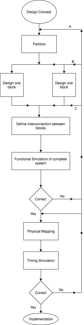
Step1: Partition circuit into smaller blocks and then design each block separately.
Step 2: After partitioning, circuitry in each block is defined and chips needed to implement it are chosen.
Step 3: After designing the blocks, the interconnection between them is defined. In this, we combine the individual blocks into a single large circuit.
Step 4: Now this complete circuit is simulated. If there are any logical errors then correct these errors.
Step 5: After completion of the functional simulation, the physical location of each chip on the board has to be determined and the wiring pattern needed to make connections between chips has to be defined.
Step 6: After physical mapping, timing simulation is performed to examine the timing behaviour of the circuit.
Step 7: After timing simulation, if everything is according to the design specifications, then the designed circuit is ready for implementation.