1. An SRAM block is a two-dimensional (2D) array of SRAM cells, where each cell can store one bit of information. If we need to store m items with n bits each, we can use an array of m × n SRAM cells.
2. The dimensions of the SRAM array are called its aspect ratio.
3. Since an SRAM block may contain a large number of SRAM cells, each cell must take as little space on an integrated circuit chip as possible. For this reason, the storage cell should use as few transistors as possible.
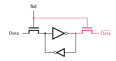
4. SRAM cell:
- Sel input is set to 1 to store data into the cell. The data value to be stored is placed on the Data input.
- The SRAM cell may include a separate input for the complement of the data.
- After waiting long enough, Sel input is changed to 0. The stored data then remains in the feedback loop indefinitely.
- Now when again Sel = 1, the value of Data may not be the same as the value being driven by the small NOT gate in the feedback path. Hence the transistor controlled by Sel may attempt to drive the stored data to one logic value while the output of the small NOT gate has the opposite logic value.
- This problem can be resolved by building the NOT gate in the feedback path using small (weak) transistors so that its output can be overridden with new data.
- To read data stored in the cell, we simply set Sel to 1. In this case, the Data node would not be driven to any value by external circuitry, so that the SRAM cell can place the stored data on this node. The Data signal is passed through a buffer and provided as an output of the SRAM block.
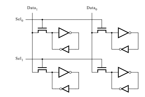
5. SRAM block:
- An SRAM block contains an array of SRAM cells.
- In each column of the array, the Data nodes of the cells are connected together.
- Each row, i of the array, has a separate select input, Seli, that is used to read or write the contents of the cells in that row.
- Larger arrays are formed by connecting more cells to Seli in each row and by adding more rows.
- The SRAM block must also contain circuitry that controls access to each row in the array.
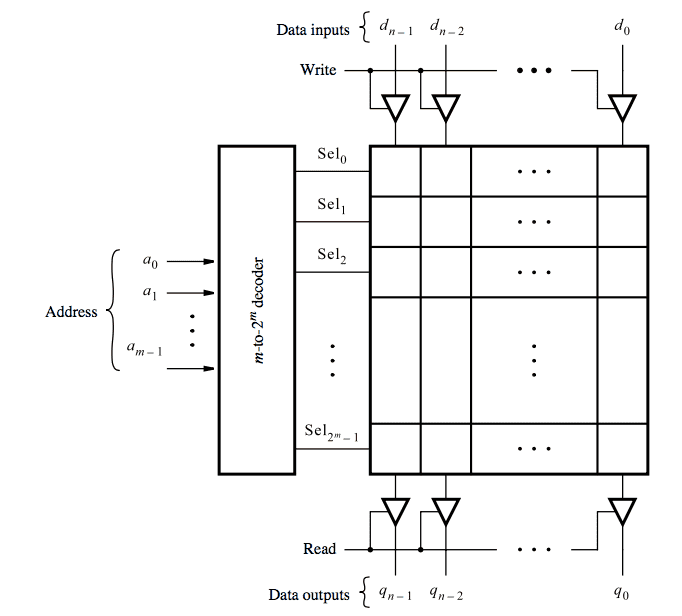
6. 2m × n SRAM block:
- It has a decoder that drives the Sel inputs in each row of the array. The inputs to the decoder are called Address inputs.
- The decoder has m Address inputs and produces 2m select outputs.
- If the Write control input is 1, then the data bits on the inputs dn−1 , . . . , d0 is stored in the cells of the row selected by the Address inputs.
- If the Read control input is 1, then the data stored in the row selected by the Address inputs appears on the outputs qn−1 , . . . , q0 .
- Practically, many a time data input(s) and data output(s) are connected together so that Write and Read inputs must never have the value 1 at the same time.
References: Fundamentals of Digital Logic with VHDL Design by Stephen Brown and Zvonko Vranesic